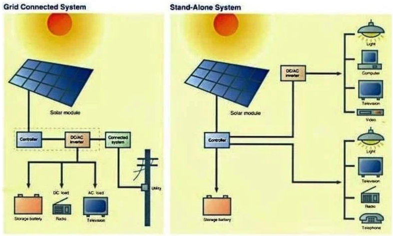
- Figure 1 – Example of Standalone system and Grid-connected system. Image courtesy of Biblus.

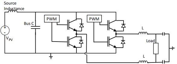
The purpose of an inverter is to transform a DC waveform voltage into an AC signal in order to inject power into a load (e.g. the power grid) at a given frequency and with a small phase angle (φ ≈ 0). A simplified circuit for a single phase unipolar Pulse-Width Modulation (PWM) is shown in Figure 2 (the same general scheme can be extended to a three phase system). In this schematic, a PV system, acting as a DC voltage source with some source inductance, is shaped into an AC signal through four IGBT switches in parallel with freewheeling diodes. These switches are controlled at the gate through a PWM signal, which is typically the output of an IC that compares a carrier wave (usually a sine wave of the desired output frequency) and a reference wave at a significantly higher frequency (typically a triangle wave at 5-20kHz). The output of the IGBTs is shaped into an AC signal suitable for use or grid injection through the application of various topologies of LC filters.

Figure 2: Pulsed Width Modulation (PWM) single-phase inverter setup. The IGBT switches, along with LC output filter, shape the DC input signal into a usable AC signal. This induces a deleterious voltage ripple across the PV terminals. The bus capacitor is sized in order to reduce this ripple.
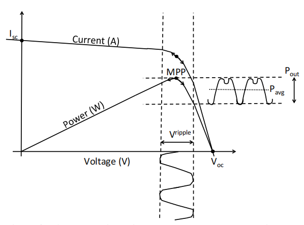
The operation of the IGBTs introduces a ripple voltage onto the terminal of the PV array. This ripple is deleterious to the operation of the PV system, since the nominal voltage applied to the terminals should be held at the max power point (MPP) of the IV curve in order to extract the most power. A voltage ripple on the PV terminals will oscillate the power extracted from the system , resulting in a lower average power output (Figure 3). A capacitor is added onto the bus in order to smooth out the voltage ripple.

Figure 3: A voltage ripple introduced onto the PV terminals by the PWM inverter scheme shifts the applied voltage off the max power point (MPP) of the PV array. This introduces a ripple in the power output of the array so that the average output power is lower than the nominal MPP
The amplitude (peak to peak) of the voltage ripple is determined by the switching frequency, PV voltage, bus capacitance, and filter inductance according to:

where:
VPV is the solar panel DC voltage,
Cbus is the capacitance of the bus capacitor,
L is the inductance of the filter inductors,
fPWM is the switching frequency.
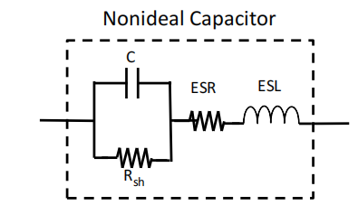
Equation (1) applies to an ideal capacitor that prevents charge from flowing through the capacitor during charging and then discharges the energy located in the electric field with no resistance. In reality, no capacitor is ideal (Figure 4) but is composed of multiple elements. In addition to the ideal capacitance, the dielectric is not perfectly resistive and a small leakage current flows from the anode to cathode along a finite shunt resistance (Rsh), bypassing the dielectric capacitance (C). When current through the capacitor is flowing, the pins, foils, and dielectric are not perfectly conducting and there is an equivalent series resistance (ESR) in series with the capacitance. Finally, the capacitor does store some energy in the magnetic field, so there is an equivalent series inductance (ESL) in series with the capacitance and ESR.

- CRE solution
CRE is a high-tech enterprise speciallizing in the production of film capacitors,focusing on application of power electrionics.CRE offer the mature solution of film capacitor series for PV inverter which including DC-link, AC-filter and snubber.
Media Contact
Company Name: Wuxi CRE New Energy Technology Co., Ltd.
Email: Send Email
Country: China
Website: https://www.cre-elec.com/
