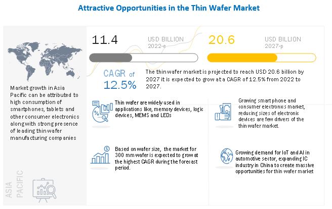
The report “Thin Wafer Market by Wafer Size (125 mm, 200 mm, and 300 mm), Process (Temporary Bonding & Debonding and Carrier-less/Taiko Process), Technology, Application (MEMS, CIS, Memory, RF Devices, LED, Interposer, Logic) and Geography – Global Forecast to 2027” The thin wafer market is projected to grow from USD 11.4 billion in 2022 and is projected to reach USD 20.6 billion by 2027; it is expected to grow at a CAGR of 12.5% from 2022 to 2027. Rise in the adoption of MEMS technology in portable health monitoring devices coupled with reduction in the sizes of electronic devices, growing smartphone and consumer electronics markets as well a high amount of material saving is expected to fuel the growth of the thin wafer market.
• Informational PDF Brochure :- https://www.marketsandmarkets.com/pdfdownloadNew.asp?id=255706993
Browse 123 market data Tables and 45 Figures spread through 197 Pages and in-depth TOC on “Thin Wafer Market and Geography – Global Forecast to 2027” View detailed Table of Content here – https://www.marketsandmarkets.com/Market-Reports/thin-wafer-market-255706993.html

Thin wafer market for LED application expected to witness the highest growth during the forecast period.
The LED application segment is likely to exhibit the highest growth during the forecast period owing to its increasing demand across the globe. Earlier, LEDs were developed through GaN; however, due to the high cost involved in the development of LED through GaN, manufacturers shifted toward thin silicon wafers. A thin wafer offers high conductivity and electrical benefits for LED chips as well as inhibits the optimal utilization of LED chips, which is not possible through GaN. These benefits of thin wafers are expected to drive market growth.
300 mm wafers expected to grow at the highest CAGR during the forecast period.
A high growth in the use of 300 mm wafers in applications like LED on account of greater yield offered by these wafers is propelling the growth of the thin wafer market across the world. It has become highly imperative for LED manufacturers to achieve economies of scale and improve profitability, which is offered by these wafers. These wafers offer manufacturers the ability to produce many devices in a single batch. This is one of the reasons companies are developing semiconductor devices that are composed of 300 mm wafers. Moreover, the rise in the number of 300 mm wafer fabrication facilities is expected to generate a significant rise in demand for 300 mm wafers.
Wafer dicing technology to dominate the market during the forecast period.
Wafer dicing dominated the thin wafer market in 2021 and is expected to follow the trend during the forecast period. The increasing demand for high-speed dicing along with superior breakage strength is contributing to the market growth. Additionally, the requirement for smaller, high performing, and less costly device configuration for use in applications such as memory devices, logic devices, power devices, and sensors is expected to contribute toward the growth of the wafer dicing equipment market during the forecast period.
Logic application to hold a significant share of the thin wafer market during forecast period.
The demand for logic devices such as microprocessors and digital signal processors is driven by growth in the implementation of server and data center systems across various businesses and industries due to the high penetration of affordable cloud computing solutions. In logic devices, thinning technology is preferred to achieve high-speed processing and reconfiguration. To ensure efficient thermal management and optimize performance, thin wafers are increasingly being used in these devices, thereby contributing to the growth of the thin wafer market for logic device’s
Americas held significant share of thin wafer market in 2021 and is expected to follow the trend by 2027
Americas is expected to account for a significance of the thin wafer market during the forecast period. The growth of the market can be attributed to the presence of key semiconductor device manufacturers and their fabrication plants in the country. This region is home to many semiconductor companies. Other than extensive globalization, the entry of global players into the region is one of the major reasons for the market growth in the Americas. The growth of the thin wafer market in the region can be attributed to the huge adoption of high-end smartphones, wearables, smart home systems, and automotive communication systems. These devices use thin wafers to minimize power losses and enable the designing of advanced architecture with high system efficiency and greater power density.
Key players in the thin wafer market include Shin-Etsu Chemical Co., Ltd. (Japan), SUMCO Corporation (Japan), GlobalWafers Co., Ltd. (Taiwan), Siltronic (Germany), SK Siltron (South Korea), SUSS MicroTec (Germany), Soitec (France), DISCO Corporation (Japan), 3M (US), and Applied Materials (US). Apart from these, Mechatronic Systemtechnik (Austria), Synova (Switzerland), EV Group (Austria), Wafer Works Corporation (Taiwan), Atecom technology Co., Ltd. (Taiwan), Siltronix Silicon Technologies (France), LDK Solar (China), UniversityWafer, Inc. (US) are among a few emerging companies in the thin wafer market.
Media Contact
Company Name: MarketsandMarkets™ Research Private Ltd.
Contact Person: Mr. Aashish Mehra
Email: Send Email
Phone: 18886006441
Address:630 Dundee Road Suite 430
City: Northbrook
State: IL 60062
Country: United States
Website: https://www.marketsandmarkets.com/Market-Reports/thin-wafer-market-255706993.html

